Ever wondered what the RTT is over PCI Express ? or you may be asking wtf is PCIe RTT ?
PCIe is quite similar to ethernet in the sense its a packet bus, where as PCI and PCI-X are the older more traditional style parallel bus. The oversimplified way to look it is, inside your PC/Server is a small ethernet network with an MTU of 128B. Could rant about PCIe quite a bit but suggest an excellent write up here to see how it all works.
By PCIe RTT it means the time to ping/pong a packet from one EndPoint (think ethernet IP) to some other EndPoint and back again. The same as an ICMP ping to some IP address. How do you write such a test ? ... with an fpga of course!
Xilinx`s Virtex 7 has a variety of SKU`s having between 1-4 PCIe Gen3 interfaces at 8 lines wide @ 8 GT/sec (note GT == Giga Transactions not GBytes). Thus the test is simply replying to an appropriately addressed PCIe TLP packet.
For the more visually inclined it looks like
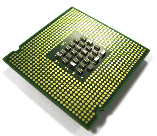
Things to note are the i7 4771 is intels latest and greatest CPU with a native PCIe Gen3 interface wired directly to the CPU pads/pins. Also note this is all "Desktop" grade hardware tho... significance of this is debatable.
And what do the numbers look like ? ..... Pretty shity actually, surprisingly shitty infact.
Above is a plot of the RTT in nanosecconds. X axis is sample count Y axis is nanos. You can see its ~ 850ns for the full Round trip... quite high to be honest. Time to dig in and investigate wtf the time has gone - and yes the card is in the correct PCIe slot!
Why so high? here`s a short list of ideas
- V7 PCIe end point
- 1337 ping code
- Intel PCIe EP
- Intel Memory Model
The easiest of these is my "1337 ping code" as the code is already in a development style setup thus getting Waves (waveforms) is straight forward.
Above is how a typical debug session goes. Run some simulation, wait a bit and check out the waves. In the above pic you can see the clock ticking over every 4ns, and 2 (out of 4) of Xilinx`s new PCIe IPCore interfaces. They are the m_axis_cq_* signals and m_axis_rq_* signals. The CPU`s register writes show up on the m_axis_cq_* interface, while our writes (to CPU`s DDR) are issued on the s_axis_rq_* interface. If you want to dig deeper check out the spec
We can then count the number of cycles between receiving the CPU write (yellow line), and the first cycle of the "1337 ping code" write into CPU DDR (red line). Which is ~16 cycles where the interface is running at 250mhz means 4ns * 16 cycles = 64ns - not particularly great but workable. Meaning the search for the remaining ~800ns remains .... inconclusive.
.... next up will investigate writing directly into the CPU`s L2 cache from the fpga, thus avoiding any shenanigans involving the CPU`s DDR.

